
A potential Apple–Intel partnership, paired with Intel’s latest process milestone, has jolted the market conversation about where the world’s most valuable compute gets built. This piece lays out what actually changed, what remains rumor, and how any deal could ripple through AI supply chains.
You’ll learn the near-term versus long-term implications for foundries, packaging, and AI hardware availability, plus practical ways to frame the trade without chasing headlines. We also connect the dots to decentralized compute and Web3 infrastructure.
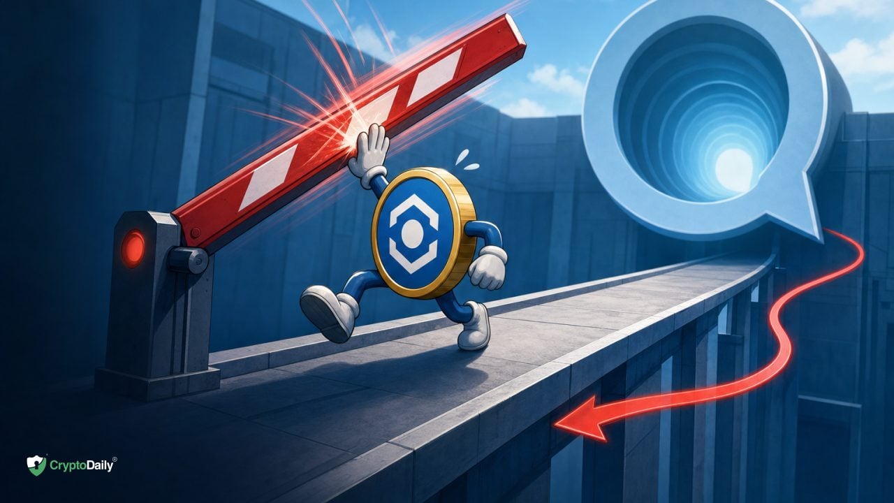
Bottom line: one announcement can sway sentiment fast—but it takes years, not weeks, to re-route silicon supply chains.
One deal can move the narrative and second‑order trades quickly, but it won’t rewrite AI hardware supply in the short run. If Apple genuinely places advanced-node volume with Intel, it could validate U.S. onshoring, pressure pricing, and diversify risk away from single‑foundry dependence. The gating items are yields, packaging capacity, and formal customer commitments; until those are visible, expect volatility more than structural change.
- Intel said its 18A‑P node has entered risk production, a key precursor to external customer ramps (The Next Web).
- A Trump post claimed Apple will work with Intel on U.S. chips; companies hadn’t confirmed at time of writing (Business Insider).
- Intel shares spiked roughly 8.8%–11% intraday after the post, underscoring sensitivity to supply‑chain headlines (Business Insider).
- Even with a marquee customer, advanced-node ramps typically hinge on yields, tool installs, and packaging queues—timelines measured in quarters to years.
What exactly changed this week, and what is verified?
Intel told attendees at the VLSI Symposium that its performance‑enhanced 18A‑P process entered risk production on June 16–17, 2026—an early, low‑volume validation phase on real silicon intended to de‑risk future customer volume (The Next Web). The company added that 18A‑P targets about 9% higher performance at the same power, or roughly 18% lower power at the same performance versus 18A, alongside thermal and design‑flexibility improvements (same source).
Separately, on June 18, 2026, President Donald Trump posted on Truth Social that “Apple has agreed to work with Intel to design and build its Chips in America,” reigniting chatter around earlier reports of Apple–Intel foundry talks. As of this writing, neither company has formally confirmed the claim (Business Insider quoting the post).
Markets reacted instantly: Intel’s stock jumped roughly 8.8% premarket and spiked intraday to about +11% the same day, reflecting how sensitive AI‑era supply‑chain trades are to any sign of customer wins or node momentum (Business Insider).
Verified: Intel’s 18A‑P risk‑production milestone and its performance‑per‑watt claims. Unverified: a binding Apple–Intel contract, volumes, timelines, or which products would shift.
How would an Apple–Intel alignment shape AI hardware supply chains?
If Apple places meaningful advanced‑node volume with Intel, several dominoes could wobble. First, it would de‑risk U.S. onshoring by anchoring a top‑tier customer to a domestic node, potentially catalyzing more ecosystem investment in EDA, IP libraries, substrates, and advanced packaging around Intel’s footprint. Second, diversifying away from a single foundry can improve negotiating leverage and resilience against geopolitical disruptions.
For AI, the direct link is nuanced. Apple’s leading‑edge silicon is mobile and PC‑centric today, while AI training demand revolves around accelerators and HBM supply. Still, a marquee customer can accelerate everything from mask‑set learning curves to packaging capacity build‑outs that benefit a broader set of chips, including AI inference parts and custom silicon.
There’s also the “software gravity” effect. If Intel’s design kits, tool flows, and libraries mature under pressure from a demanding customer, other customers can onboard faster. That compresses go‑to‑market time for both consumer SoCs and AI‑adjacent ASICs.
But the plumbing matters: packaging (e.g., 3D stacking), substrate lead times, and HBM assembly remain bottlenecks industry‑wide. Customer wins don’t bypass physics or factory cycle times; they justify more capex to expand those pipes.
Where does this leave TSMC, Samsung, and Nvidia right now?
TSMC remains the incumbent for Apple’s M‑series and for most bleeding‑edge AI accelerators, with mature 3nm production and a deep advanced‑packaging bench. Samsung is aggressively pushing its advanced nodes and 3D packaging to win back premium mobile and compute share. Nvidia’s supply still depends on foundry capacity, HBM availability, and advanced packaging slots—areas where TSMC’s scale has been decisive.
If Intel converts interest into volume, expect pricing pressure and more multi‑sourcing, but incumbents won’t relinquish share easily; yield leadership, packaging throughput, and ecosystem tooling often matter more than headline node names.
Vendor/Node Status (mid‑2026) Performance/Power Angle Advanced Packaging Notable Customer Exposure Intel 18A‑P Risk production announced (June 16–17, 2026) ~9% perf at same power or ~18% lower power vs 18A (company claim) Foveros/EMIB for 2.5D/3D integration Positioned to serve external foundry customers; Apple rumored, not confirmed TSMC 3nm family In mass production Iterative efficiency/performance gains vs 5nm/4nm nodes CoWoS/SoIC widely used for high‑end AI parts Apple (M‑series), Nvidia and other leading designers Samsung advanced nodes Competing at 3nm and below Focused on power efficiency and PPA competitiveness X‑Cube and 3D stacking initiatives Premium mobile, compute, and foundry customers
Interpret the table qualitatively: Intel’s milestone is real but early; TSMC’s production footing and packaging scale still dominate today’s AI accelerator ramps; Samsung is the wildcard for customers seeking a second source at leading nodes.
What would it take for Intel to win meaningful Apple volume?
Apple tends to prize performance‑per‑watt, reliability, and supply certainty. To displace any portion of existing foundry allocations, Intel must meet or exceed targets not only on transistor metrics, but also in design ecosystem maturity, packaging quality, and delivery schedules.
In practice, that means the following diligence for anyone assessing feasibility in the next 12–24 months.
- Yield trajectory: Look for consistent, improving yields on complex SoCs through multiple mask spins—not just test vehicles.
- EDA and IP readiness: Robust PDKs, verified libraries, and smooth tool flows minimize time‑to‑tapeout headaches.
- Packaging throughput: High‑volume, advanced 3D stacking with predictable thermals and warpage control.
- Cost and pricing: Competitive wafer and packaging economics at scale, including long‑term agreements.
- Supply assurance: Clear capacity roadmaps, redundancy, and logistics to meet peak product cycles.
- Confidentiality and co‑development: Secure environments for custom features without IP leakage.
Only when multiple boxes are ticked does large‑scale migration become plausible. Until then, partial allocations or product‑specific splits (for example, by SKU or by region) are more realistic than a full‑stack switch.
How should AI‑focused investors reframe the trade?
When headlines break, first separate signal from sentiment. Risk production and rumored design wins move multiples, but bottlenecks—like HBM, substrates, and packaging—govern shipments. Price action often overreacts to rumor and underprices slow‑burn capacity changes.
Consider the stack of potential beneficiaries if U.S. onshoring gains traction: equipment makers (lithography, deposition, etch), substrate suppliers (ABF), OSAT/advanced packaging specialists, EDA software vendors, and specialty materials. These categories can benefit from capex and capacity expansions, regardless of which foundry captures the flagship logo.
For designers and hyperscalers, more credible second sources can compress lead times and improve price discovery. But near‑term AI accelerator availability still hinges on HBM output and packaging slots—both constrained, and both requiring multi‑year investments to ease.
Pro tip: In AI hardware trades, focus on the slowest‑moving bottleneck. Over the past cycles that’s been advanced packaging and HBM, not front‑end wafer starts. Leadership there tends to accrue the most durable pricing power.
What is the crypto and Web3 angle here?
Decentralized compute markets, AI‑adjacent GPU networks, and even some Bitcoin miners pivoting to AI workloads all face the same upstream constraints: GPU/ASIC supply, HBM availability, and packaging. If U.S. onshoring expands real capacity—especially in packaging—it could eventually lower lead times and reduce geographic concentration risk for these networks.
For Web3 projects offering verifiable AI inference or decentralized rendering, domestic capacity can also mean clearer compliance paths and improved latency for U.S. users. That said, onshoring doesn’t remove export‑control frictions or the premium pricing that comes with leading‑edge capacity in tight markets.
Token prices tied to “AI compute” narratives may react to macro silicon news, but fundamentals depend on delivered throughput, uptime, and cost per inference. Watch actual hardware installations and service‑level metrics rather than headlines.
What risks could derail this narrative?
Risk production is not risk‑free. It’s a necessary milestone, not mass production. Yields can stall, design kits can need more work, and packaging integration can slip schedules. The market often prices risk production like a de facto ramp; it isn’t.
Customer confirmation and scope matter. A public post is not a definitive supply agreement. Even with a deal, the scope could be narrow (e.g., certain SKUs or pilot runs) and may not materially dent competitor share in the first year.
Capex and cost inflation can bite. Building competitive leading‑edge capacity in the U.S. is capital‑intensive. Subsidies and incentives help, but cost structures must still close the loop at scale.
Geopolitics and export controls remain fluid. Policy shifts can affect tool shipments, customer allocations, and cross‑border workflows. Multi‑sourcing is a hedge, not a shield.
Common Mistakes
- Trading rumor as revenue: Assuming an unconfirmed partnership equals immediate multi‑billion‑dollar orders. Avoid this by waiting for company filings or capacity disclosures.
- Ignoring packaging and HBM: Focusing on wafer nodes while overlooking the binding constraints that set shipment pace. Track packaging expansions and memory supply.
- Underestimating ramp times: Expecting risk production to become volume inside a quarter. Most leading‑edge ramps require multiple quarters to stabilize yields.
- Conflating node names with performance: Marketing labels don’t guarantee PPA leadership for real‑world designs. Compare delivered perf/W and thermals by workload.
- Overlooking ecosystem maturity: Dismissing EDA, IP libraries, and tool chains that determine how fast customers can tape out and debug.
For continuing coverage of AI infrastructure, market structure, and the digital‑asset edge, visit Crypto Daily.
Frequently Asked Questions
Does risk production mean chips will ship this year?
Not necessarily. Risk production validates the process on early silicon and uncovers issues before high‑volume manufacturing. Volume depends on yields, packaging readiness, and customer tapeouts—timelines often run several quarters.
Could Apple split orders across foundries without a full switch?
Yes. Large designers often dual‑source by product line, SKU, or region. Early engagements can start with lower‑risk parts or limited runs before any flagship migration.
Will this change Nvidia GPU availability in the near term?
Unlikely in the immediate quarter. Nvidia’s availability is tied to its foundry allocations, HBM supply, and packaging slots. A potential Apple–Intel deal affects ecosystem investment but won’t instantly add capacity for Nvidia‑class accelerators.
Is Intel’s 18A‑P aimed at AI accelerators or mobile/PC SoCs?
The node targets broad, performance‑per‑watt‑sensitive designs. Whether it is used for AI accelerators, mobile, or PC silicon depends on customer choices and packaging strategies. Intel highlighted perf/W improvements versus 18A in its VLSI remarks.
How can I track whether a deal is real and material?
Watch for company confirmations, earnings call color, capital‑commitment disclosures, and evidence of tool installs or packaging expansions. Design‑win headlines without capacity signals are not definitive.
Are there ETFs that capture a U.S. onshoring theme?
Several semiconductor and manufacturing ETFs provide diversified exposure to equipment makers, foundries, and materials. Each has different weightings and risks—review holdings and concentration carefully.
What’s the single most important bottleneck to watch?
In today’s AI cycle, advanced packaging and HBM assembly remain the gating factors. Even with new front‑end nodes, shipments can’t accelerate if those back‑end stages lag.
Disclaimer: This article is provided for informational purposes only. It is not offered or intended to be used as legal, tax, investment, financial, or other advice.


 English (US) ·